- up to 20 fps speed,
- viewfinder or display blackout-free shooting,
- up to 60 AF/AE tracking calculations per second,
- silent vibration-free electronic shutter speeds up to 1/32000 sec.
- Anti-Distortion Shutter operation that minimizes distortion of moving subjects
- Full pixel array readout with no pixel binning for oversampled 4K 30p video
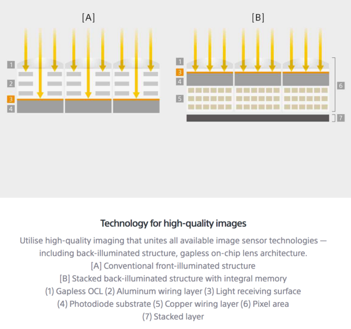
SonyAlphaRumors publishes a number of slides on the new image sensor:


"Full frame", a typo in the title.
ReplyDeleteThanks! Fixed.
ReplyDelete3rd image is just the second image with less of the text but with an added "useless" button on top left. - did i miss something? maybe some different image was meant to be posted here.
ReplyDeleteRight. Meant to be other image. Thanks!
DeleteIs this the same stack technology as the ISSCC paper in Feb, in the Experia XZ Motioneye camera?
ReplyDeleteI do not know for sure, but I don't think so. The ISSCC paper had 3 layers of silicon and in this Sony presentation I do see only 2 layers. But the device in this presentation is a very large one, so the large supporting chip can easily have memory and processing on-board without the need for an extra layer with DRAM. So after all, this presentation still may have the same functionality as the ISSCC paper, but only with two layers of silicon and not three.
DeleteIf someone has another opinion .... ???
DRAM is generally not integrated on one die with advanced logic process nodes, so unlikely that we are seeing folding of two die into one.
DeleteSony may have e-DRAM technology since I seem to remember Toshiba used to use embedded trench DRAM in some of the game processors that they made for Sony - mind you, that was quite a few years ago!
DeleteI think I've answered my own question after looking at the video - looks like a CIS/memory package stack, with a separate Bionz processor. Not a three-layer stack with TSVs.
ReplyDeleteI am not 100 % sure if you are right. On the picture they show (second one of the three), they clearly indicate a memory part together with processing on one chip. But of course you never know whether this is the exact structure in silicon as well ...
DeleteOn the other hand, it does not matter that much, after all it is a great piece of technology !!!
@Dick James - "Stacked" means more of the front-side circuitry is moved to the back; it is more "BSI" than BSI. In addition to moving some more of the circuitry from front to back they can add additional layers to enable PDAF and increase the Readout Speed.
ReplyDeleteThis Sensor is 'like' the Xperia XZ / Z Pro etc. (960 FPS Cellphone Sensor) except the DRAM is not as large (capable of such high speed) and the physical size is Full Frame (that's the "new" part, Full Frame).
See: https://www.xda-developers.com/sony-imx378-comprehensive-breakdown-of-the-google-pixels-sensor-and-its-features/ and Mark Weir of Sony: https://youtu.be/oG2UPQfPNDs?list=PLWa6uO3ZUweB_LFvUpNPoxUs-9CtqFKN0 or even Wikipedia.
The IMX400 Stacked Sensor is detailed in this Article: http://image-sensors-world.blogspot.ca/2017/05/techinsights-publishes-sony-3-layer.html .
ReplyDelete